Silicon: A Closer Look At The Material That Unleashed A Refreshing Range Of Haute Horlogerie Ideas
Following the recent article on silicon balance springs by watchmaker Ashton Tracy called Is Silicon Here To Stay In (Rolex) Watch Movements?, I wanted to take a closer look at the intriguing material from which they are made and how they are made.
Silicon is, after oxygen, the most abundant material on earth. In its pure crystalline form it is the basis of the microelectronics industry: our smart phones, televisions, and computers. And it has given its name to one of the most affluent areas in the world: California’s Silicon Valley.
The production of crystalline silicon is a fascinating process.
It takes 24-48 hours to grow the silicon cylinder from which all begins. The formation is initiated by what’s known as a seed crystal, the silicon cylinder – or “boule” – is marked with an “orientation flat.”
Silicon lies immediately below carbon in the periodic table and, as we would expect, has similar properties. It is tetravalent, meaning it likes to form links with four other atoms or ions. Pure silicon readily forms large crystals in which each silicon atom is linked to four others in what is known as a cubic lattice. This is the same lattice structural arrangement as diamond.
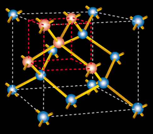
A silicon cubic lattice unit cell
Representing the crystal structure of silicon, the cube outlined in red in the depiction above has a pink silicon atom at its center linked to four others at diagonally opposite corners. Eight of these red cubes make up the “unit cell” of the silicon crystal, which readers who like mental challenges will realize contains eight atoms. (Hint: there are only four atoms wholly within the cell; the remainder is shared with adjacent cells.)
In the video above we saw that the production of the monocrystalline silicon boule is initiated by a seed crystal, which imposes its structure on the entire crystal produced so its orientation is vital.
The 100, 110, or 111 faces of silicon
Visualizing the seed crystal as a cube we can imagine touching it on the molten silicon face first, edge first, or corner first. Withdrawing it would produce respectively wafers with 100, 110, or 111 faces.
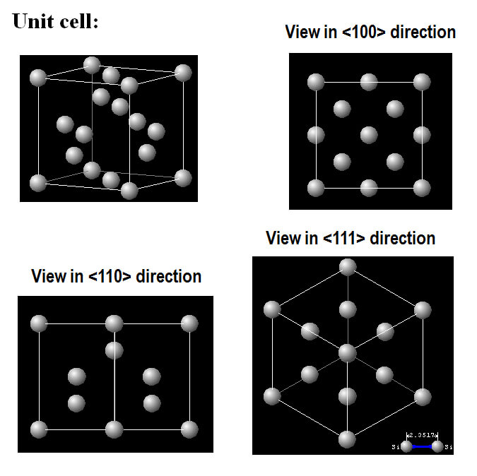
Visualizing the seed crystal as a cube with 100, 110, or 111 faces
Looking squarely at the face of the cube, we see a 100 view, with an edge facing us we see 110, and with a corner 111.
The electronics industry prefers wafers with the 100-face orientation so that is the most readily available and therefore most widely used in making components for mechanical watches.
When looking at the wafer the unit cells are arranged like boxes in a stack, all precisely aligned. They are “glued” tightly together by the chemical bonds between them. Indeed, these robust bonds exist throughout the material.
There is however a “but”: the physical properties of monocrystalline silicon – strength, elasticity, temperature response, etc. – vary with the orientation of the crystal.
The microelectronics industry relies on the electrical properties of silicon varying with orientation, but it has been suggested that in the watch industry it is mechanical properties of silicon that are paramount.
It may be better, particularly for balance springs, to be using 111-face wafers, which have six-fold symmetry. I haven’t found anyone in the industry prepared to discuss this. The problem may be largely theoretical: if the weakest link in a chain is far stronger than the demands likely to be made on it, failure is unlikely.
Masking and etching: DRIE for silicon components
Silicon watch parts, such as escapement components and balance springs, are produced by a high-tech process known as DRIE (Deep Reactive Ion Etching). This may be thought of as a form of machining: start with a piece of material, cut away what you don’t want, and you are left with what you do want.
The “cutting” is done by a very aggressive chemical process in the presence of high-energy plasma.
The steps involved are outlined in a sequence of images provided by Sigatec, one of the earliest companies in this field, and one who did pioneering work with Ulysse Nardin under previous owner Rolf Schnyder.
A photolithographic process is used to coat a silicon wafer with a mask containing silhouettes of the component to be produced. This is placed in an evacuated chamber in a powerful electric field. Sulfur hexafluoride (SF6) is introduced into the chamber, and the fluoride ions etch the silicon producing silicon tetrafluoride (SiF4).
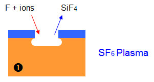
Above the silicon is shown in orange and the resistant mask in blue. Note that the etching process undercuts the edges of the mask.
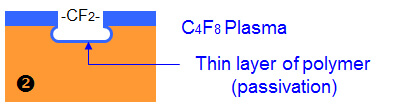
To prevent this continuing, the chamber is flushed with another gas, C4F8. This coats the surface with a PTFE-like layer (think non-stick cookware). This process is called passivation.
When the system is again flushed with SF6, etching continues. The passivation layer is attacked, and because the plasma field is directed downward the horizontal layer is removed to allow further etching. But because of the oblique angle, the edge continues to be protected.
Again there is some undercutting, so the C4F8 step is repeated. This continues for many, many cycles, each around ten seconds. Each cycle only removes fractions of a micron of silicon, so producing components, say, 150 microns thick, takes several hours.
The result of etching, viewed in an electron microscope, shows that successive cycles of etching and passivation produce straight, vertical edges with no perceptible undercutting. For lovers of acronyms, this form of the DRIE process patented by Bosch is described as TMDE (Time Multiplexed Deep Etching) and it is said to be ideal for HARS (High Aspect Ratio Structures).
Etched silicon wafer containing hundreds of silicon components destined for the Ulysse Nardin Freak’s escapement
The etched silicon wafer, at left in the photo above, shows hundreds of silicon components prior to release. In this case they are wheels for the escapement of the Ulysse Nardin Freak.
Note that it is the material around the components that is removed. The etching process has a lot of work to do.
Looking at the image of the whole wafer we see (at around 5 o’clock) the “flat” machined on the edge of the original boule. The flat presents another 100-face wafer (a cube looks the same from the side as it does from the top).
In orienting the mask, manufacturers take care to maintain the same relationship with this flat, ensuring that the properties of the components are the same from batch to batch.
Reflecting wavelengths for color
Silicon components can be extraordinarily colorful; literally, all the colors of the rainbow are possible. This is because, post-production, as movie makers would say, they are oxidized in a furnace.
A glass-like layer of amorphous Si02 (silica), which is formed on the surface, breaks up the light falling on it, reflecting different wavelengths according to its thickness. A variety of colors are seen in images of silicon components used in a high-frequency concept watch by Chopard.
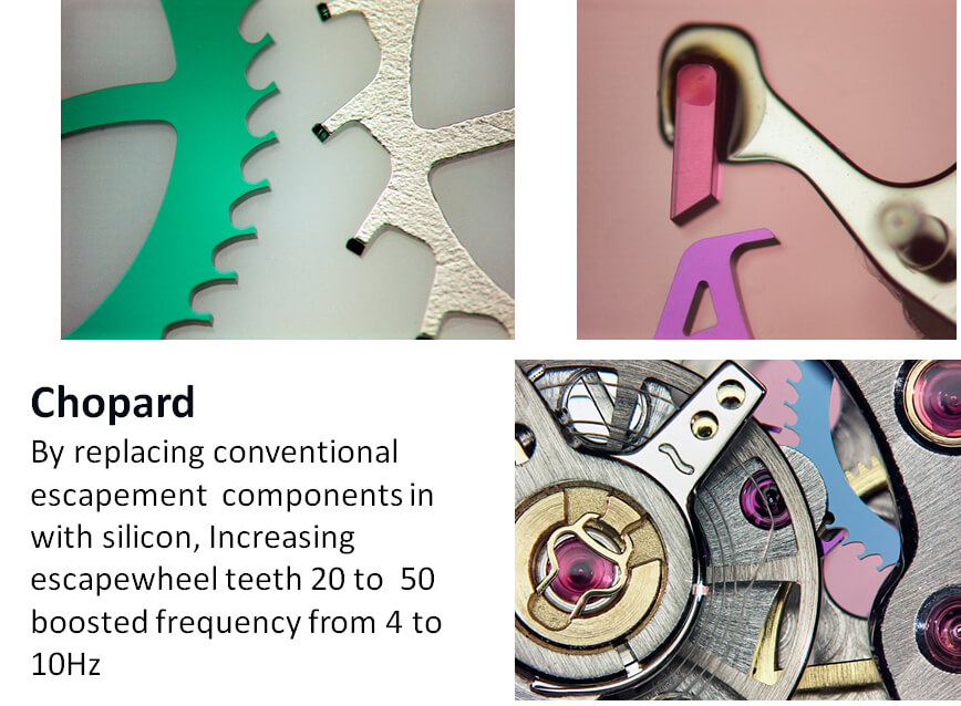
A variety of colors in silicon components used in a high-frequency concept watch by Chopard
Here silicon components are compared with the conventional equivalents. They appear green, magenta, and blue.
Again, silicon’s key proponents in the watch industry have been completely uncooperative in revealing the thickness and purpose of this layer but readily available data indicates that it provides a harder surface with a lower coefficient of friction.
The thermal expansion coefficient of silicon is small, and a coating of silicon dioxide reduces it further.
Components made with silicon
By using silicon the same sized escape wheel can have many more teeth, acting on a finer anchor that doesn’t need pallets.
Patek Philippe has, for one, also patented Silinvar, an oxidized silicon used in the Spiromax balance. “Silinvar” is a combination of words, “invar” being the name given to a nickel-iron alloy used for pendulum rods.
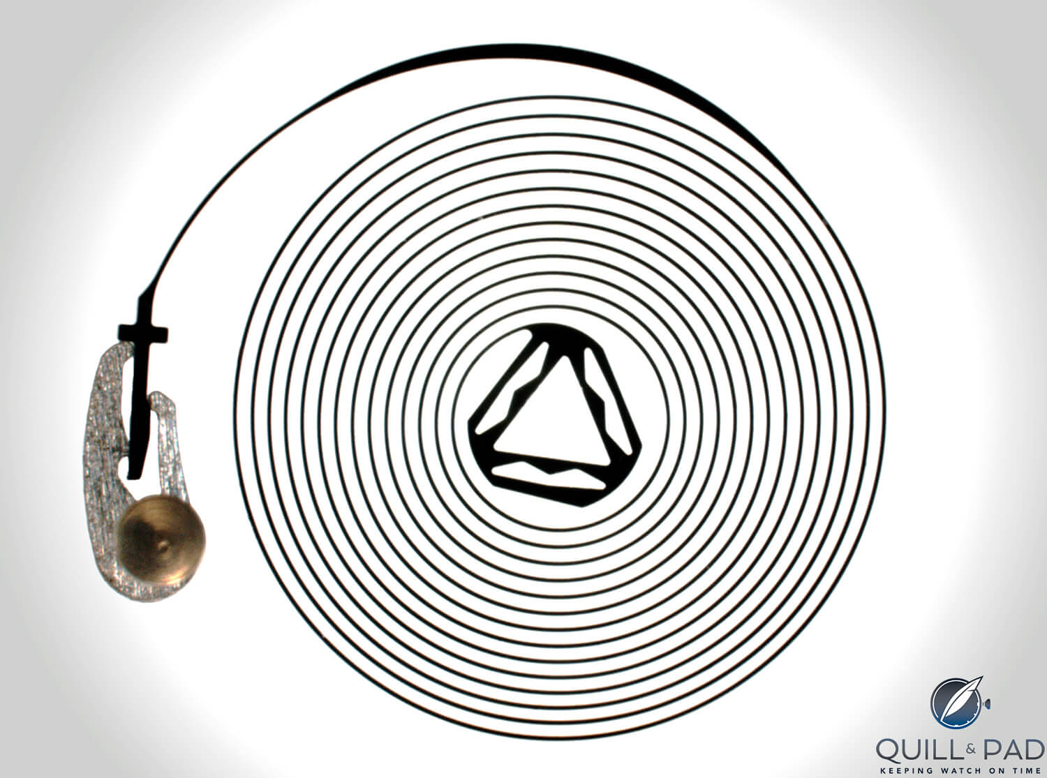
Patek Philippe Spiromax silicon balance spring
A metal spring is a spiral of uniform material. In the Spiromax we have, in one piece, a springy central triangle allowing an unambiguous attachment to the balance staff, and a uniform spiral slightly thickened towards the outer end to mimic the effect of an overcoil, terminating in a T-shaped piece that can be fitted, again unambiguously, to the stud.
Sadly, Patek Philippe would not respond to detailed questions about the nature of Silinvar. Reduced to guessing, I would imagine that the thermal properties of the dioxide would not predominate unless they were the major component.

Having looked at the detailed structure of silicon components, I should also highlight important physical properties that make it an excellent material for use in mechanical watches.
As mentioned by Ashton, silicon is completely non-magnetic, a property watchmakers have been seeking for many years. Breguet’s magnetically supported balance staff could not be used without it.
Silicon is less than a third the density of conventional materials, greatly reducing inertia. This is particularly important in the “stop/go” components in watch escapements. Moreover, parts made of conventional materials are often more massive than their function requires because they must be able to withstand the rigors of the production process – being scraped by a cutting tool.
The dimensions of a silicon component can be reduced to that required by its function, making them still lighter.
Silicon’s critics mention that it is brittle. A dictionary tells us brittle means “breaks easily.” This is not the technical meaning.
A brittle material will remain elastic up to the point where the load exceeds its elastic limit and it fractures. Being brittle means that if it bends or stretches when under load, it will return to its former shape when the load is removed. Provided the elastic limit is not exceeded it’s an ideal structural material, particularly for springs.
The case for silicon is perhaps best exemplified by the extraordinary one-piece component produced for Girard-Perregaux’s genuinely constant-force escapement, because it could not have been produced in any other way.
Virtually any flat object you can draw can be made from silicon using DRIE. This has unleashed a refreshing range of ideas taking us far beyond haute horlogerie’s penchant for merely miniaturizing traditional pocket watch complications.
You might also be interested in:
Is Silicon Here To Stay In (Rolex) Watch Movements?
Give Me Five! All 5 Of Patek Philippe’s Advanced Research Limited Editions
Trackbacks & Pingbacks
-
[…] O silício tem vindo aos poucos a revolucionar o mundo da relojoaria, principalmente, ao nível dos componentes mecânicos. E é com toda a pertinência, face ao atual contexto da relojoaria, que aqui deixamos um artigo bem composto sobre este material. Sendo assim, falamos de uma abordagem ao nível da sua composição, das suas implicações e o modo como tem vindo a ser utilizado no mundo da mecânica relojoeira. Para ler no sempre obrigatório Quill & Pad. […]
Leave a Reply
Want to join the discussion?Feel free to contribute!


Great article.
Just a precision about oxidation and Silinvar. Silinvar is just Patek’s commercial name of a process that was developed and patented by a consortium composed of CSEM (a Swiss science institute), Rolex, Patek and Swatch Group. The idea of the patent is that silicon has an elasticity which increases with temperature, and silicon oxyde has one which diminishes. So if you have the right proportion of each, you can have an elasticity which does not vary with temperature.
Thanks for that further detail. The extent of oxidation, the ratio of the oxide to the metal, which would be very interesting to know, remains a mystery. Does anyone have a broken silinvar spring they can examine? (probably not)
To speak more frankly, this CSEM claim that the temperature response of silicon and its oxide differ in sign, one positive and the other negative, made at the time Silinvar was announced, is one that I can’t find any justification for in the literature. No effect like it has ever been reported in the available literature. Could the report have been an error? Is this why Patek won’t respond to questions?